Cactus Materials
Home
Products: Chips
Applications
Foundry
News
Team
Contact
Home
Products: Chips
Applications
Foundry
News
Team
Contact
Search
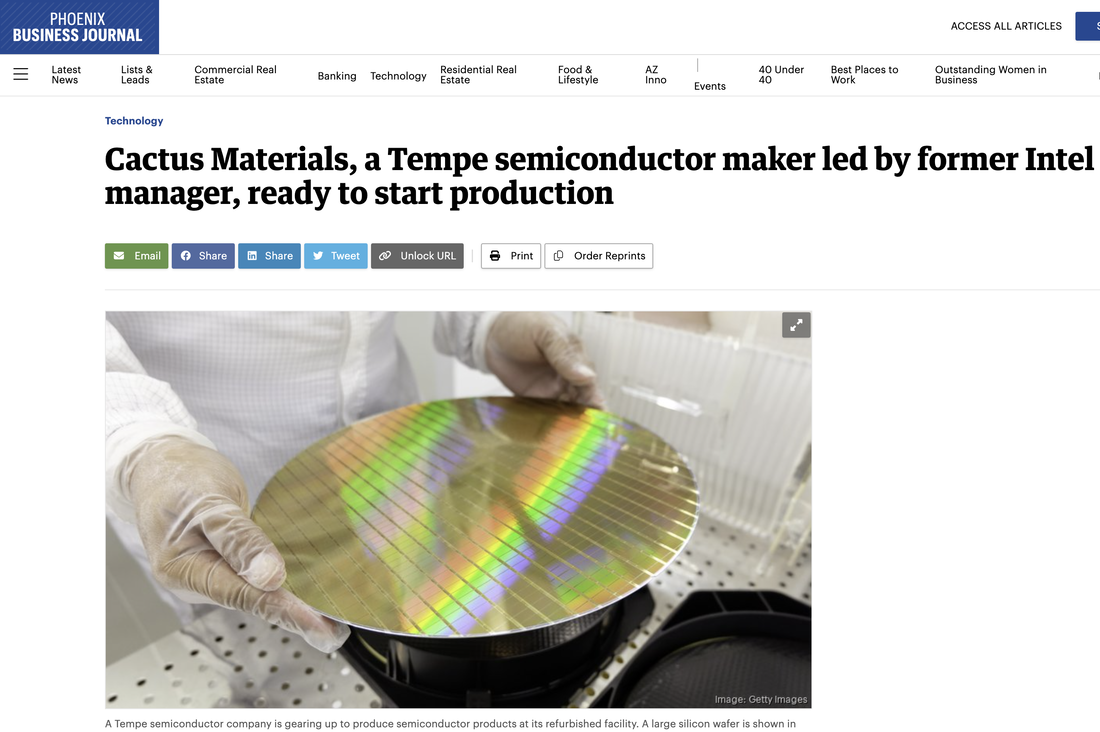
Cactus Materials, a Tempe semiconductor maker led by former Intel manager, ready to start production
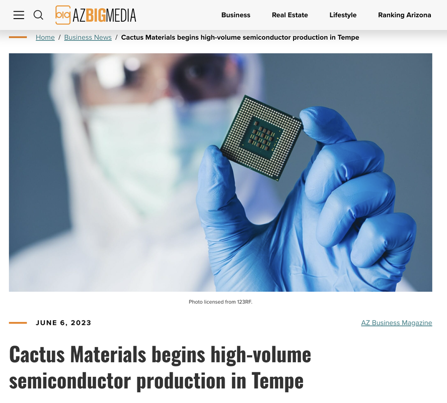
Cactus Materials begins high-volume semiconductor production in Tempe
Workshop brings academic, industry partners together to collaborate on CHIPS Act projects
Southwest Advanced Prototyping Hub
Key Conferences:
How can we help you?
*
Indicates required field
Name
*
First
Last
Email
*
Comments
*
Company Name
*
Phone Number
*
Submit
Cactus Materials, Inc.
2507 W Geneva Drive
Tempe, AZ 85282
[email protected]
Home
Products: Chips
Applications
Foundry
News
Team
Contact